Microfluidic
Cartridge &
Chip Manufacturing
Precision thermoplastic fabrication with Class 100K cleanroom assembly. From prototypes to high-volume production with scalable bonding solutions.
Request Technical ConsultationCustomer Challenges
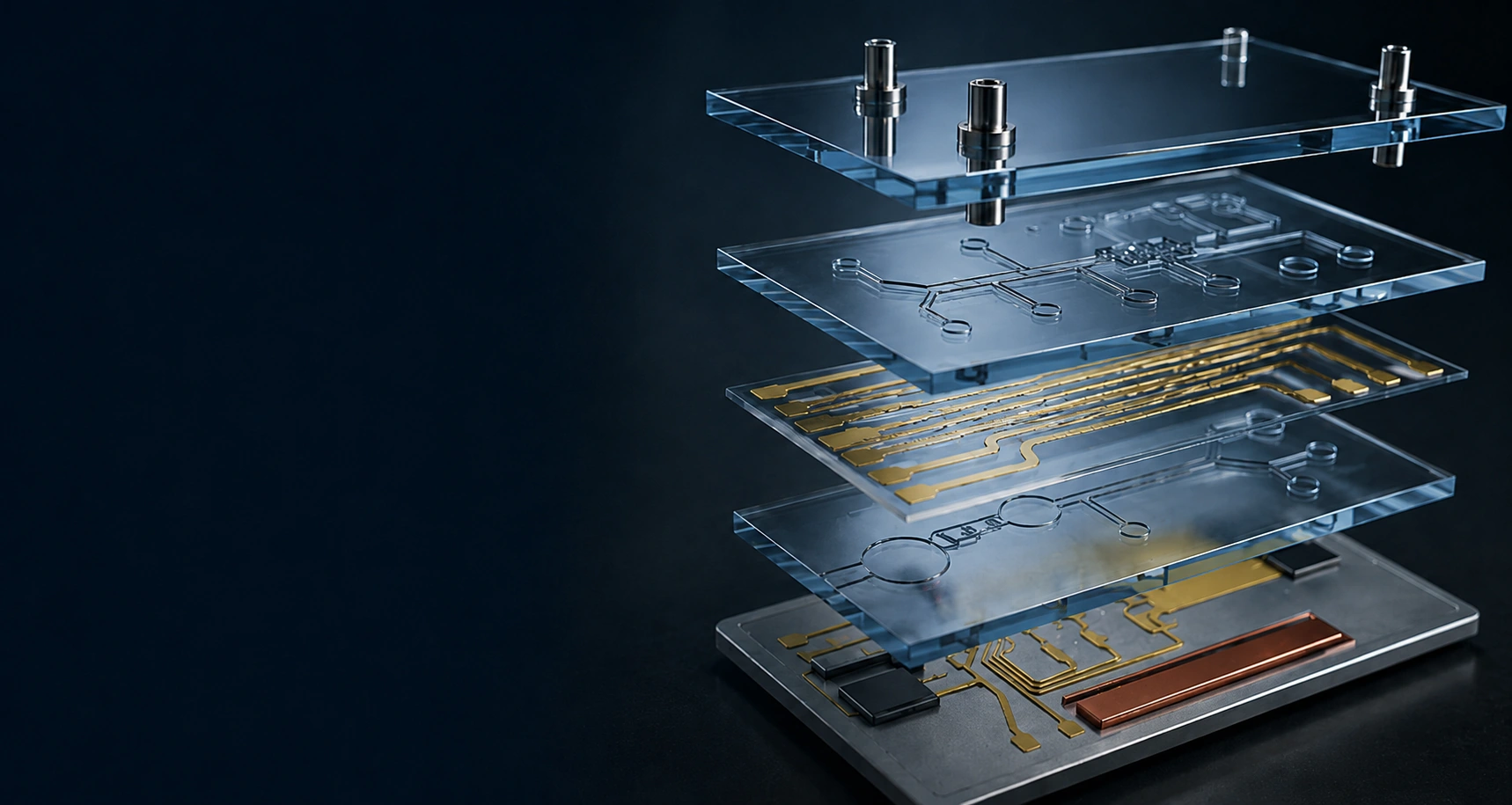
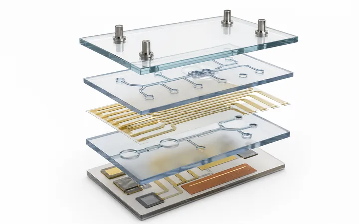
Customers designing microfluidic cartridges need plastic layers, microchannels, embedded functional elements, and cleanroom assembly to work together without leaks, distortion, or inconsistent performance.
Layer Alignment
- Two plastic layers must register accurately
- Channels must stay open after bonding
- Warpage can shift critical interfaces
- Design must be manufacturable at volume
Bonding Integrity
- Seals must hold without blocking channels
- Thermal and ultrasonic windows can be narrow
- Transparent devices need cosmetic control
- Leak paths must be designed out early
Embedded Functions
- Electrodes, membranes, sensors, or reagents must fit the cartridge stack
- Interfaces need protection from process stress
- Materials must remain chemically compatible
- Assembly cannot introduce contamination
Scale & Traceability
- Prototype choices must translate to production
- Cleanroom packout must be repeatable
- Flow and leak checks need defined criteria
- Quality records must support customer validation
Fu Yu Strategic Approach
Our approach answers those customer challenges with DFM support, precision thermoplastic moulding, controlled bonding, functional integration, and verified cleanroom assembly.
DFM Before Tooling
We review gate placement, channel orientation, layer registration, bonding land, and interface risks before customers commit to tooling.
Precision Moulded Layers
Thermoplastic moulding controls channel geometry, optical areas, and mating surfaces so the bonded stack starts from stable parts.
Controlled Bonding Window
Thermal, ultrasonic, or solvent bonding is selected around material compatibility, seal strength, channel openness, and cosmetic needs.
Integration & Verification
Embedded electrodes, membranes, reagents, and sensors are protected through assembly, then verified through leak, flow, visual, and traceability checks.
7-Step Process
From design to delivery, our comprehensive workflow ensures quality
Channel Design
Precision channel geometry optimization for fluid dynamics and manufacturing feasibility
Thermoplastic Moulding
High-precision injection moulding with material selection for optimal bonding compatibility
Surface Prep
Critical surface treatment protocols for maximum bond strength and reliability
Bonding Method
Selection and execution of optimal bonding technique based on application requirements
Functional Integrations
Integration of sensors, valves, and other components during bonding process
Leak / Flow Verification
Comprehensive testing protocols to ensure hermetic sealing and proper flow characteristics
Cleanroom Packout
ISO-certified cleanroom packaging and documentation for immediate deployment
DFM Checklist
Top customer-facing DFM checks before tooling and scale-up.
Gate Placement
Gate and knit-line planning for clear channels and stable fill
Channel Orientation
Layer registration and channel direction matched to use case
Warpage Control
Flatness control so bonded layers seal without distortion
Membrane Interfaces
Membrane, electrode, sensor, and reagent interface planning
Optical Clarity
Material selection for transparency
Reagent Compatibility
Chemical resistance validation
DFM Checklist for Microfluidics
Design for manufacturability guidelines to ensure successful production scaling from prototype to high-volume manufacturing.
- Channel width ≥50µm for injection moulding
- Aspect ratio <3:1 for reliable demoulding
- Draft angles 0.5-2° for vertical walls
- Minimize sharp corners (R≥25µm)
- Gate location away from critical features
- Bonding area ≥2mm for reliable sealing
Risk Register & Mitigation
Common failure modes and our proven mitigation strategies for robust microfluidic device production.
Mitigation: Optimized bonding parameters, leak testing protocols
Mitigation: Surface treatment, adhesion promoters
Mitigation: Surface coatings, optimized channel geometry
Mitigation: Material selection, controlled processing
Mitigation: USP Class VI materials, validated processes